CXA2525AM
Description
112k 124 44k 8 44k 112k 124 9 8 9 11 E F TE I I O 124 11 320k 73.4k Tracking error amplifier input for Pins 8 and 9; tracking error drive output for Pin 11. 120 25 10 10 VC O 120 (VCC + GND) / 2 DC voltage output. 348k 12 FE O 348k 124 12 Focus error amplifier output for Pin 12. 13 RFO_2 O 124 14 13 Buffer switch output which sets the RF signal time constant. OFF when Pin 19 is connected to VCC, ON when it is connected to GND. 1k 14 17 RFO_1 RF_M O I 124 17 2k 14 Non-inversion input of RF drive amplifier for Pin 17; RF signal output for Pin 14; resistance value connected between Pins 14 and 17 which determines the low frequency gain of RF drive amplifier. -4- CXA2525AM/AN Pin No.
Key Features
- Wide-band RF amplifier. (RF signal fc ≥ 12MHz)
- RF equalizer (T type)
- EFM time constant can be adjusted (with switching function)
- APC (Automatic Power Control) function
- Power saving function Functions
- RF summing amplifier
- RF equalizer
- Focus error amplifier
- Tracking error amplifier
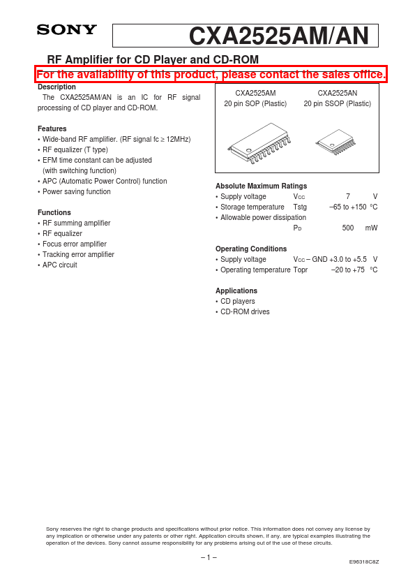
- APC circuit CXA2525AM 20 pin SOP (Plastic) CXA2525AN 20 pin SSOP (Plastic)